General Description
The RTQ2103A is a full featured 6V, 2A, Advanced Constant-On-Time (ACOT®) synchronous step-down converter with two integrated MOSFETs. The advanced COT operation allows transient responses to be optimized over a wide range of loads, and output capacitors to efficiently reduce external component count. This document explains the function and use of the RTQ2103A evaluation board (EVB) and provides information for the evaluation board layout, schematic, bill of materials (BOM) and measurement results to suit individual requirements.
Performance Specification Summary
Summary of the RTQ2103AGSP-QA Evaluation Board performance specificiaiton is provided in Table 1. The ambient temperature is 25°C.
Table 1. RTQ2103AGSP-QA Evaluation Board Performance Specification Summary
|
Specification
|
Test Conditions
|
Min
|
Typ
|
Max
|
Unit
|
|
Input Voltage Range
|
|
3
|
--
|
6
|
V
|
|
Output Current
|
|
0
|
--
|
2
|
A
|
|
Default Output Voltage
|
|
0.45
|
--
|
3.3
|
V
|
|
Operation Frequency
|
|
2200
|
2700
|
3000
|
kHz
|
|
Output Ripple Voltage
|
VIN = 3.3V, VOUT = 1.2V, IOUT = 2A
|
--
|
10
|
--
|
mVp-p
|
|
Line Regulation
|
IOUT = 0A, VIN = 3V to 6V
|
--
|
±1
|
--
|
%
|
|
Load Regulation
|
VIN = 3.3V, VOUT = 1.2V, IOUT = 1mA to 2A
|
--
|
±1
|
--
|
%
|
|
Load Transient Response
|
IOUT = 650mA to 1.37A
|
--
|
±5
|
--
|
%
|
|
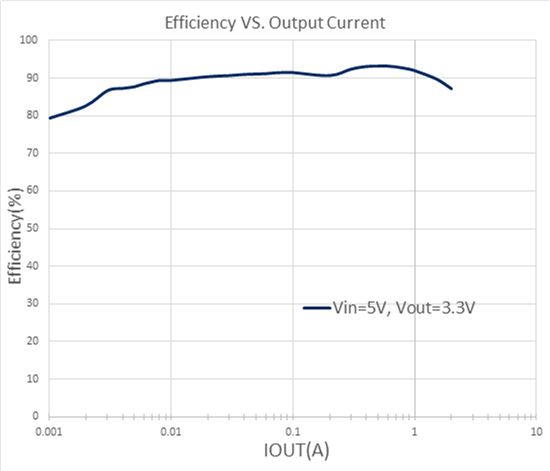
Maximum Efficiency
|
VIN = 5V, VOUT = 3.3V, IOUT = 0.5A
|
--
|
93.2
|
--
|
%
|
Power-up & Measurement Procedure
1. Apply a 5V nominal input power supply (3V < VIN < 6V) to the VIN and GND terminals.
2. Set the jumper at JP1 to connect terminals 1 and 2, connecting EN to enable operation.
3. Verify the output voltage (approximately 3.3V) between VOUT and GND.
4. Connect an external load up to 2A to the VOUT and GND terminals and verify the output voltage and current.
Output Voltage Setting
Set the output voltage with the resistive divider (R24, R29) between VOUT and GND with the midpoint connected to FB. The output is set by the following formula:
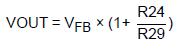
The placement of the resistive divider should be within 5mm of the FB pin. The resistance of R29 is suggested between 10kΩ and 150kΩ to minimize power consumption, and noise pick-up at the FB pin. The resistance of R24 can then be obtained as below:
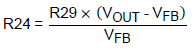
For better output voltage accuracy, divider resistors (R24 and R29) should have tolerance of ±1% tolerance or better.
Detailed Description of Hardware
Headers Description and Placement
Carefully inspect all the components used in the EVB according to the following Bill of Materials table, and then make sure all the components are undamaged and correctly installed. If there is any missing or damaged component, which may occur during transportation, please contact our distributors or e-mail us at evb_service@richtek.com.
Test Points
The EVB is provided with the test points and pin names listed in the table below.
|
Test point/
Pin name
|
Signal
|
Comment (expected waveforms or voltage levels on test points)
|
|
EN
|
Enable Test Point
|
Chip enable. Externally pulled high to enable and pulled low to disable this chip.
|
|
PGND, GND
|
Power Ground
|
The exposed pad must be soldered to a large PCB and connected to PGND for maximum power dissipation.
|
|
AGND
|
Analog Ground
|
Should be electrically connected to GND close to the device.
|
|
FB
|
Feedback
|
Feedback voltage input.
|
|
VOS
|
Output Voltage Sense
|
Output voltage sense pin for the internal control loop. Must be connected to output.
|
|
PG
|
Power Good Test Point
|
Output of power good indicator.
|
|
SW
|
Switch Node Test Point
|
Switch node.
|
|
VIN
|
Input Voltage
|
Power input.
|
Bill of Materials
|
Reference
|
Qty
|
Part Number
|
Description
|
Package
|
Manufacturer
|
|
U4
|
1
|
RTQ2103AGSP-QA
|
DC-DC Converter
|
PSOP-8
|
RICHTEK
|
|
C10, C14
|
2
|
GRM188R71H104KA93D
|
0.1µF/50V/X7R
|
0603
|
MURATA
|
|
C11
|
1
|
GRM32E61E226KE15L
|
22µF/25V/X5R
|
1210
|
MURATA
|
|
C12
|
1
|
|
NC
|
1206
|
|
|
C13
|
1
|
C3216X5R1H106KT000N
|
10µF/50V/X5R
|
1206
|
TDK
|
|
C15
|
1
|
|
NC
|
1206
|
|
|
C31
|
1
|
|
NC
|
0603
|
|
|
L1
|
1
|
PST25201B-1R0MS
|
1µH
|
2x2.5x1.2mm
|
CYNTEC
|
|
R24
|
1
|
WR06X6532FTL
|
249k
|
0603
|
WALSIN
|
|
R29
|
1
|
WR06X3922FTL
|
39.2k
|
0603
|
WALSIN
|
|
R30
|
1
|
WR06X1003FTL
|
100k
|
0603
|
WALSIN
|
|
R31
|
1
|
WR06X1803FTL
|
180k
|
0603
|
WALSIN
|
|
CP1
|
1
|
|
Short
|
|
|
Typical Applications
EVB Schematic Diagram
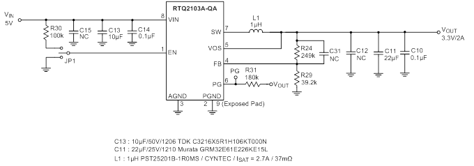
Note :
1. Do not hot-plug a live 5V supply to the board; if hot-plugging is required, add ~100µF electrolytic capacitor at the input.
A small feedforward capacitor (C31) can be introduced into the feedback network to speed up the transient response of high output voltage circuits. Adding C31 can also improve the light load PSM switching behavior. The feedforward capacitor is added across the upper FB divider.
To optimize transient response, C31 value is chosen so that the gain and phase boost of the feedback network increases the bandwidth of the converter, while still maintaining an acceptable phase margin. Generally, larger C31 values provide higher bandwidth, but may result in an unacceptable phase margin or instability.
Measurement Results
|
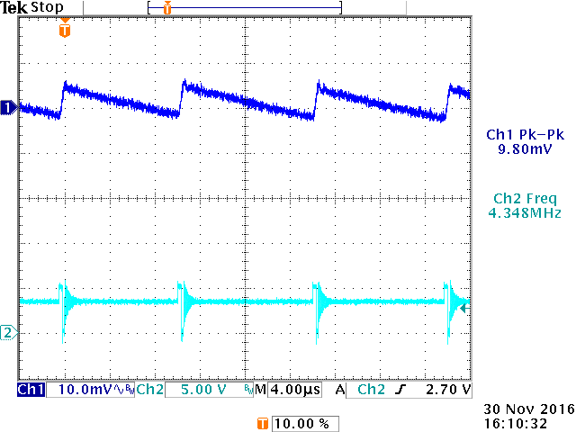
Output ripple measurement, 10mA load
Cyan: V-SW; Blue: VOUT
|
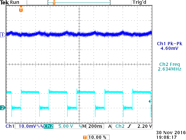
Output ripple measurement, 2A load
Cyan: V-SW; Blue: VOUT
|
|
|
|
|
Output ripple: 9.8mVpp (PSM mode)
|
Output ripple: 4.6mVpp, Frequency: 2.634MHz
|
|
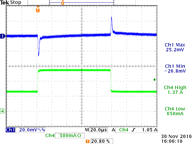
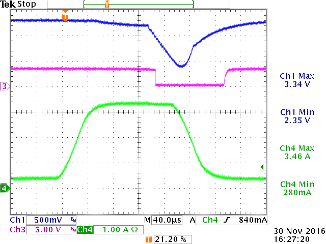
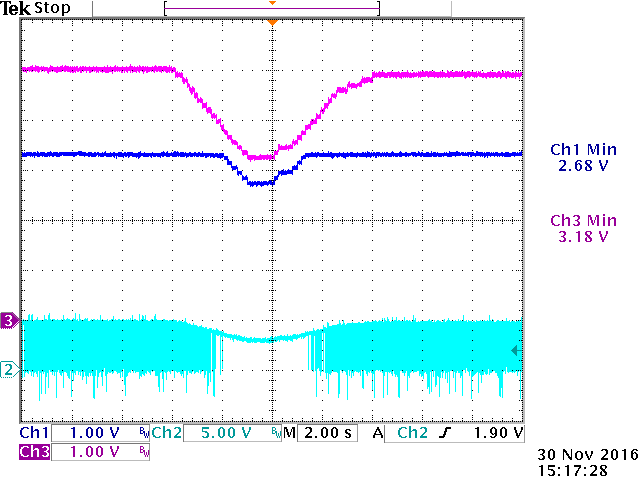
Dynamic load 650mA to 1.37A (PWM)
Blue: VOUT; Green: Load current step
|
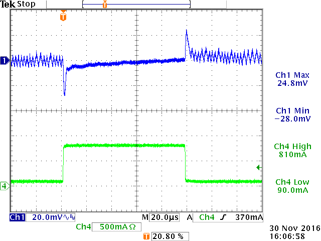
Fast dynamic load 90mA to 810mA
(PSM – PWM transition)
Blue: VOUT; Green: Load current step
|
|
|
|
|
Overshoot: 25.2mV, undershoot: 26.8mV
|
Overshoot: 24.8mV, undershoot: 28mV
|
|
OCP measurement: Dynamic load close to OCP
Blue: VOUT; Purple: PGOOD; Green: IOUT
|
OCP measurement:
Increase load current to reach OC limit
Blue: VOUT; Purple: PGOOD; Green: IOUT
|
|
|
|
|
V-out starts to drop at 3.46A load current
|
Auto-recovery hiccup mode when OC limit is exceeded
|
|
Start-up measurement from Enable: EN pin low – high
Cyan: V-Enable; Blue: VOUT; Purple: PGOOD; Green: IOUT
|
Start-up measurement from VIN
Cyan: VIN; Blue: VOUT; Purple: PGOOD; Green: IOUT
|
|
|
|
|
Start-up time 304µsec. Soft-start 224µsec
|
VIN > 2.4V initiates start-up
|
|
100% Duty cycle test
Cyan: V-SW; Blue: VOUT; Purple: VIN
|
|
|
Efficiency Measurements
5V to 3.3V
|
VIN (V)
|
VOUT (V)
|
IIN (A)
|
IOUT (A)
|
Efficiency (%)
|
|
4.99896
|
3.30416
|
0.00084
|
0.00101
|
79.4
|
|
4.99982
|
3.30873
|
0.00376
|
0.00498
|
87.7
|
|
4.99951
|
3.31045
|
0.00738
|
0.00997
|
89.4
|
|
4.99876
|
3.32859
|
0.03655
|
0.05001
|
91.1
|
|
4.99914
|
3.31526
|
0.07247
|
0.10001
|
91.5
|
|
5.00026
|
3.30779
|
0.21491
|
0.30016
|
92.4
|
|
4.99888
|
3.31052
|
0.35531
|
0.50022
|
93.2
|
|
4.99927
|
3.31346
|
0.49902
|
0.70030
|
93
|
|
4.99959
|
3.31701
|
0.72110
|
1.00040
|
92
|
|
5.00025
|
3.32051
|
1.10942
|
1.50068
|
89.8
|
|
5.00018
|
3.32091
|
1.52368
|
2.00095
|
87.2
|
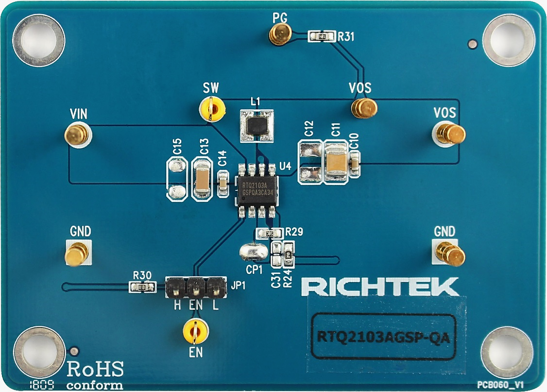
Evaluation Board Layout
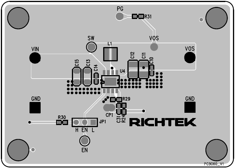
Figure 1. Top View
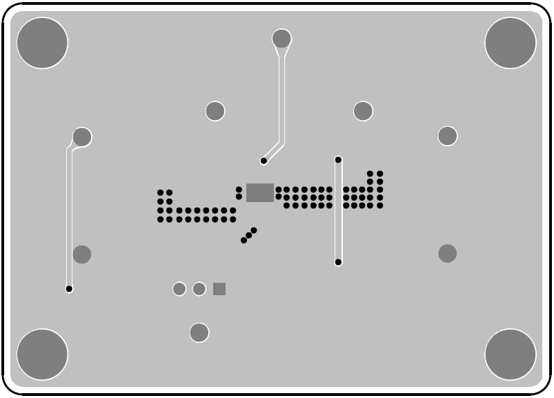
Figure 2. Bottom View